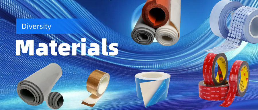

To implement EMI shielding in your PCB design, you should select the right shielding materials, optimize your board layout, and use advanced solutions like our EMI Shielding Foam. You protect your devices from unwanted electromagnetic interference and ensure they meet strict industry standards. Effective EMI shielding helps you maintain device performance, prevent signal loss, and achieve regulatory compliance in demanding environments.
Key Takeaways
- Choose the right materials and optimize your PCB layout to reduce electromagnetic interference and improve device performance.
- Use proper grounding methods and shielding materials like our EMI Shielding Foam to protect circuits from EMI and meet industry standards.
- Design your PCB with careful trace spacing, impedance matching, and component placement to minimize noise and signal loss.
- Leverage die-cutting expertise to get custom-fit EMI shielding foam parts that simplify installation and enhance reliability.
- Test and validate your EMI shielding early and often using simulation tools and EMC testing to ensure compliance and long-term device stability.
EMI Shielding Basics
What is EMI?
Electromagnetic interference (EMI) is unwanted energy that disrupts the normal operation of electrical circuits. You encounter EMI when external sources—such as lightning, radio transmitters, or malfunctioning electronics—emit electromagnetic waves that interfere with your devices. EMI can take several forms:
- Radiated EMI: Travels through the air and affects devices at a distance.
- Conducted EMI: Moves along electrical paths like wires or power lines.
- Coupled EMI: Transfers through induction or capacitance, even without direct contact.
Industry standards, including CISPR, FCC Part 15, IEC 61000, and MIL-STD-461, define how you should measure and control EMI. These standards require you to test for both emissions and susceptibility, ensuring your devices do not cause or suffer from harmful interference. Managing EMI is essential for device reliability and regulatory compliance.
Tip: EMI can come from both natural sources, like solar flares, and human-made sources, such as cellphones or industrial equipment.
Impact on PCB Design
EMI directly affects how you design printed circuit boards (PCBs). When traces on your PCB run too close together, crosstalk can occur. Crosstalk is unwanted noise caused by capacitive and inductive coupling between conductors. This noise degrades signal integrity and can lead to device malfunction.
You can reduce EMI by increasing the spacing between traces, shortening conductor lengths, and providing multiple return paths for signals. Tight coupling of signal traces with their reference planes also helps minimize field spreading. Advanced simulation tools, such as Altium Designer’s Signal Integrity feature, allow you to predict and address crosstalk before manufacturing.
Statistical trends show that effective EMI Shielding depends on both material properties and design choices. Shielding effectiveness (SE) is measured by how well a material reflects and absorbs electromagnetic waves. Materials with SE values above 30 dB are considered efficient, and optimizing impedance matching further improves performance. By understanding these principles, you can create robust PCB designs that meet industry standards and perform reliably in real-world environments.
Causes of EMI
Common Sources
You face many sources of electromagnetic interference in modern PCB designs. Power supplies, wireless transmitters, and high-speed digital circuits often generate strong electromagnetic fields. Motors, relays, and switching regulators also contribute to EMI in industrial and consumer devices. Even everyday items like LED drivers or USB chargers can introduce unwanted noise.
A comprehensive study shows that near-end crosstalk (NEXT) and far-end crosstalk (FEXT) are the most common EMI sources in today’s high-density PCB applications. These issues appear most often in audio, multimedia, and smart handheld devices where traces run close together and follow random paths. Researchers used both experimental measurements and advanced electromagnetic field modeling to confirm that crosstalk between traces dominates EMI in these environments. Their findings highlight the importance of careful trace routing and layout planning to reduce interference.
Note: EMI can also come from external sources, such as radio towers or nearby electronic equipment. Shielding and proper grounding help protect your circuits from these outside threats.
Design Factors
Your PCB layout decisions play a major role in controlling EMI. Several design metrics directly impact how much interference your board generates or receives:
- Impedance discontinuities can cause overshoot and ringing, which increase radiated emissions.
- Crosstalk between adjacent traces becomes a problem if you do not maintain at least three times the trace width as spacing.
- Reflections and ringing often result from unmatched impedances.
- Via stubs and poor trace layout can degrade signal integrity.
- Common-mode currents may rise due to electric coupling between power and ground planes.
- Differential pair routing helps reduce noise by canceling out common-mode signals.
- The choice between surface-mount and leaded components affects EMI performance.
- Improper PCB layout and component placement can create unintended antennas, increasing EMI.
Simulation tools and frequency response measurements confirm that these factors influence EMI levels. You can minimize interference by matching impedances, designing multi-layer stack-ups, and arranging components thoughtfully. Careful planning at the design stage leads to more reliable and compliant electronic products.
Shielding Techniques
Grounding and Layout
You can significantly reduce electromagnetic interference by focusing on grounding and PCB layout. Proper grounding strategies form the backbone of EMI Shielding in any electronic design. You should use star grounding, which connects all grounds to a single point. This method minimizes ground loops and prevents EMI noise from circulating through your system. Chassis grounding, where you connect the circuit ground to a metal enclosure, helps dissipate unwanted energy.
Many engineers also avoid ground loops by carefully planning the ground paths. Ferrite beads and common-mode chokes suppress high-frequency noise on both power and signal lines. Filtering techniques, such as low-pass filters and EMI filters, block unwanted high-frequency signals before they reach sensitive components.
Tip: Multi-point grounding and hybrid grounding (a combination of single-point and multi-point) have proven effective in reducing EMI. Grounding grids offer low-impedance paths for current, further improving your board’s immunity to interference.
Case studies show that optimizing grounding topology can resolve EMI failures in medical devices and aerospace systems. You can achieve robust EMI Shielding by combining these grounding strategies with careful component placement and trace routing. Simulation tools and EMC testing help you verify the effectiveness of your layout before production.
Shielding Materials
Selecting the right materials is crucial for effective EMI Shielding. You have several options, each with unique properties and trade-offs. The table below compares common materials used in PCB shielding:
| Material | Advantages | Disadvantages |
|---|---|---|
| Copper | Excellent EMI shielding due to high conductivity | Heavier and more costly |
| Aluminum | Lightweight and good conductivity | Less effective than copper, may need thicker layers |
| Nickel | Good corrosion resistance and effective EMI blocking | Lower conductivity compared to copper and aluminum |
| Conductive Paint | Cost-effective and easy to apply | Less effective, requires multiple layers for optimal shielding |
You should also consider material certifications and test standards. For example, MIL-DTL-83528C specifies shielding effectiveness ratings for elastomeric gaskets, while ASTM D4935-10 and IEEE-299-2006 provide standardized test methods for measuring shielding effectiveness across a wide frequency range. Independent labs like MET Labs and Eurofins E&E North America use these standards to certify materials, ensuring your design meets industry requirements.
Testing in semiconductor and PCB manufacturing confirms that metal layers, ground planes, and advanced composites can achieve high EMI Shielding effectiveness. For instance, composite films with silver-coated microspheres or nanowires have demonstrated shielding effectiveness values above 80 dB, providing strong protection for sensitive circuits.
Enclosures and Cans
Physical barriers such as enclosures and shielding cans play a vital role in EMI Shielding. You can use metal enclosures to act as Faraday cages, blocking external electromagnetic fields from reaching your PCB. Shielding cans, which you solder directly over sensitive components, provide localized protection.
Experimental studies show that shielding cans reduce coupling between components, especially below the first resonant frequency of the enclosure. However, you must carefully design these cans to avoid resonance issues, which can amplify energy inside the cavity and reduce shielding effectiveness. Simulation software helps you predict and address these effects before finalizing your design.
Note: Always pay attention to seams, vias, and openings in your enclosures. Even small gaps can allow EMI to leak through, so use conductive gaskets or EMI Shielding Foam to seal these areas.
Comprehensive EMI testing, including the use of reverberation chambers and standardized test plans, ensures that your enclosures and cans deliver the required level of protection. By combining robust grounding, the right materials, and well-designed enclosures, you can achieve reliable EMI Shielding and meet regulatory standards.
EMI Shielding Foam
Product Features
The EMI Shielding Foam stands out because of its advanced engineering and strict quality standards. You benefit from a product that delivers reliable performance in demanding environments. Here are the key features you should know:
- Holds ISO9001, ISO14001, and IATF 16949 certifications, ensuring consistent quality and responsible manufacturing.
- Delivers high shielding effectiveness, with SE values often exceeding 90 dB for excellent EMI protection.
- Offers excellent conductivity due to advanced fillers like silver-coated aluminum and pure nickel.
- Maintains long-term stability, resisting rust, wear, and moisture even in harsh conditions.
- Meets fire safety and eco-friendly requirements, complying with RoHS and other green standards.
- Provides a wide range of material options, including beryllium copper, stainless steel, conductive rubber, conductive fabrics, and BandSorb® absorbing materials for broad frequency coverage.
- Undergoes advanced testing using ion beam spectroscopy, electron microscopy, and Vector Network Analyzers to verify shielding, reflection, and absorption performance.
You can trust the EMI Shielding Foam to protect your devices and support compliance with industry regulations.
Die-Cutting Process
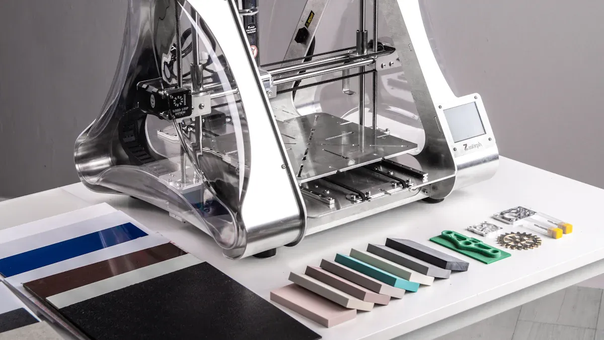
We brings over 20 years of die-cutting expertise to every project. You receive foam components that fit your exact design requirements. The process starts with material selection based on your application’s needs. Our engineers design precise cutting molds to match your PCB layout.
You benefit from advanced flatbed and rotary die-cutting machines. These machines create clean, accurate cuts, even for complex shapes or small parts. We can add features like punched holes or conductive adhesives to meet your unique installation needs. Every piece undergoes strict quality checks to ensure it meets your specifications.
Our die-cutting process guarantees that each EMI Shielding Foam part integrates seamlessly into your assembly, saving you time and reducing installation errors.
Application and Customization
You can use the EMI Shielding Foam across many industries. Automotive electronics, aerospace systems, portable devices, military equipment, medical devices, and industrial automation all benefit from tailored EMI solutions. ODT works closely with you to understand your project requirements and deliver prototypes quickly.
Customization options include:
- Selecting the right foam thickness and material for your frequency range.
- Designing parts to fit around connectors, chips, or enclosures.
- Adding conductive adhesives for easy installation.
- Optimizing the foam’s microstructure for better impedance matching and wave attenuation.
We supports you through every step, from design consultation to installation guidance. You receive detailed instructions to maximize shielding performance. If you need help with testing or validation, our team provides technical support and documentation.
With the EMI Shielding Foam, you achieve reliable EMI protection, long-term durability, and compliance with environmental standards—all tailored to your specific application.
Best Practices
Material Selection
Choosing the right materials for your PCB design directly impacts EMI performance. You should focus on materials with low dielectric constant and minimal signal loss, especially for high-frequency applications. Materials like Teflon (PTFE) and ceramic help reduce EMI by maintaining signal integrity. For environments with high temperatures, polyimide and ceramic offer excellent thermal stability. If you work with medical devices, biocompatibility and durability become essential for long-term reliability.
| Material | Dielectric Constant (εr) | Loss Tangent (tan δ) | Cost |
|---|---|---|---|
| FR4 | 4.3-4.7 | 0.02-0.03 | Low |
| Rogers RO4003C | 3.38 | 0.0027 | Medium |
| Teflon (PTFE) | 2.1 | 0.0002 | High |
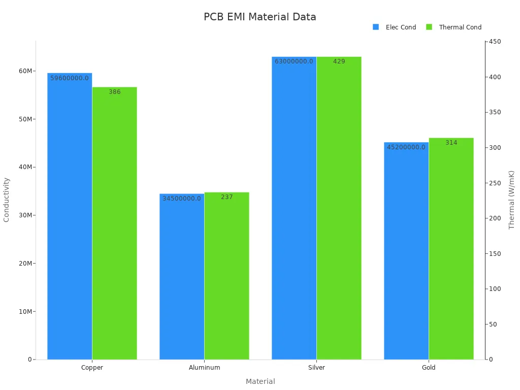
Materials with superior electrical conductivity, such as copper and silver, further enhance EMI performance. The chart below compares electrical and thermal conductivity for common PCB materials:
Integration Tips
You can minimize EMI by following proven layout strategies:
- Use controlled impedance routing to maintain signal quality.
- Apply proper grounding techniques to reduce noise.
- Utilize differential signaling for better noise immunity.
- Place decoupling capacitors near power pins to stabilize voltage.
- Space traces generously and avoid parallel routing.
- Use solid power and ground planes for shielding.
- Separate analog and digital grounds.
- Employ guard fences around sensitive components.
- Stack signal layers next to ground planes.
- Add series termination resistors to dampen reflections.
- Group components by signal type.
- Use surface mount devices to lower inductance.
- Maintain trace spacing using the 3W rule.
- Route differential pairs closely.
- Avoid 90° bends; use 45° bends.
- Minimize vias to reduce EMI.
Tip: Careful integration of these techniques ensures your EMI Shielding remains effective throughout the product lifecycle.
Testing and Validation
You should validate your EMI Shielding approach at every stage of development. Use simulation tools like SPICE and full-wave electromagnetic simulators early in the design process. Conduct EMC testing in specialized chambers to measure radiated and conducted emissions. Simulate EMI conditions and measure interference levels to identify and address weak points. Quantitative measurements confirm the effectiveness of your shielding and layout strategies. Iterative testing and validation help you achieve reliable operation and regulatory compliance.
You can achieve robust EMI Shielding in your PCB designs by selecting quality materials, optimizing layouts, and using advanced solutions like the EMI Shielding Foam. When you follow these steps, you help your products pass critical tests, such as EMC emission, insulation resistance, and thermal safety. The die-cutting expertise ensures each component fits perfectly and supports eco-friendly manufacturing. Apply these best practices to boost device reliability and meet industry standards.
- Pass EMC emission and immunity tests for regulatory compliance.
- Complete insulation and leakage current tests for safety.
- Verify thermal and overcurrent protection for long-term reliability.
FAQ
What is the main benefit of using EMI Shielding Foam in PCB design?
The material offers high shielding effectiveness, long-term durability, and compliance with industry standards. You can customize it for your specific application.
How do you install EMI Shielding Foam on your PCB?
You place the die-cut foam over sensitive areas or between enclosures and components. We provides installation guidance and can add conductive adhesives for easy application.
Can you use EMI Shielding Foam in harsh environments?
Yes. The foam resists rust, moisture, and wear. It maintains performance in automotive, aerospace, and industrial settings. You can trust it for long-term stability.
What industries benefit most from EMI Shielding Foam?
You see strong results in:
- Automotive electronics
- Aerospace systems
- Medical devices
- Consumer electronics
- Industrial automation
How do you verify the effectiveness of EMI shielding in your design?
You use simulation tools and EMC testing to measure emissions and immunity. We supports you with technical documentation and testing guidance to ensure your design meets regulatory standards.