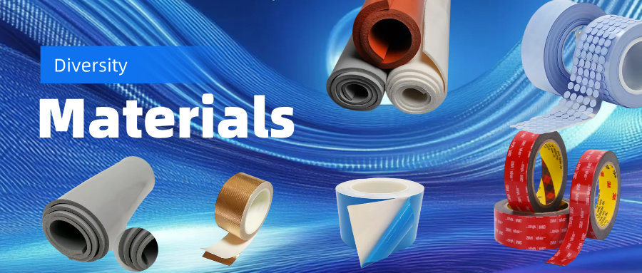

Die Cut Thermal Pad are soft, thermally conductive interface materials used to transfer heat between uneven or irregular surfaces—especially between electronic components (like chips, power modules) and heat sinks or metal chassis. These materials are designed to “fill the gap” where air would otherwise act as a poor thermal conductor.

?Key Characteristics in Detail
High Thermal Conductivity
Thermal gap pads are loaded with ceramic or metallic particles (like alumina, boron nitride, or aluminum oxide) that provide efficient heat transfer, typically ranging from 1 to 10 W/m·K, depending on the application.Soft and Conformable
Their softness (measured in Shore 00 or Shore A hardness) allows them to compress and conform to surface irregularities—even if the contact areas are uneven or rough. This ensures full surface contact for better heat transfer.Electrical Insulation
Most gap pads are electrically non-conductive, providing dual functionality: thermal transfer and electrical isolation. This is critical when pads are placed between high-voltage components and grounded heat sinks.Vibration Damping
The elastomeric nature of the pads helps absorb vibration or shock, reducing mechanical stress on components over time—especially important in automotive or industrial settings.Customisable Formats (Die-Cut Ready)
They can be produced in sheets, rolls, or pre-cut custom shapes using die-cutting techniques, enabling precise placement in assembly lines and compatibility with automated pick-and-place systems.
Why Are Die Cut Thermal Pad Important?

? Working Principle:
Electronic components like CPUs or IGBT modules generate heat. To maintain performance and avoid thermal failure, this heat must be transferred efficiently to a cooling solution. However, no two surfaces are perfectly flat; microscopic gaps exist between components and heat sinks.
If left unaddressed, these gaps are filled with air—one of the worst thermal conductors.
Thermal gap pads replace air pockets with a material that conducts heat much better, reducing thermal resistance (measured in °C·cm²/W) and maintaining component temperature within safe limits.
Real-World Applications

1. Consumer Electronics
In smartphones, tablets, and laptops, processors and memory modules are densely packed in small spaces. Thermal gap pads are used to transfer heat from the chips to metal frames or heat spreaders without damaging delicate components.
2. Automotive Electronics
Electric vehicles (EV) use power control units, inverters, and onboard chargers—all of which generate significant heat. Die Cut Thermal Pad help manage this heat while also accommodating mechanical stress caused by road vibrations and thermal cycling.
3. LED Lighting
LED lose efficiency and lifespan if they overheat. Gap pads fill the space between the LED module and heat sink, enabling compact lighting solutions with effective thermal management.
4. Telecommunication Equipment
Base stations, 5G antenna units, and network routers rely on thermal gap pads to ensure the continuous operation of high-speed chips in tightly packed environments.
Material Structure and Properties
? Composition Breakdown:
Polymer Base:
Typically silicone, thanks to its flexibility, temperature stability (up to 200°C), and long-term durability. For silicone-sensitive environments (e.g., optical or camera modules), acrylic or urethane-based gap pads are used instead.Filler Particles:
Thermally conductive but electrically insulating materials such as alumina (Al₂O₃), boron nitride (BN), or aluminum nitride (AlN). The choice of filler determines the thermal conductivity, mechanical properties, and dielectric strength.Reinforcement Layers (Optional):
Some pads include fiberglass or film reinforcements to improve tear strength during assembly, especially for thin or high-compression applications.
Die-Cutting in Thermal Gap Pad Production

Thermal gap pads are often produced in bulk and then die-cut into custom shapes. Die-cutting enhances efficiency in high-volume production and simplifies manual or robotic installation.
✂️ Common Die-Cutting Techniques:
Kiss Cut (Half Cut):
Cuts through the thermal pad but not the release liner. Pads remain on a roll or sheet, ideal for automated peeling and placement.Through Cut (Full Cut):
Cuts completely through both material and liner. Used for packaging individual pieces or when manual application is preferred.Rotary Die Cutting:
Suitable for high-volume runs with consistent quality. Offers tight tolerances, often ±0.1mm, which is critical in electronics assembly.Laser Cutting:
Used for prototyping or when extremely fine features are required. However, it may cause slight discoloration or hardened edges depending on the material.
Trends, Innovations & Challenges

? Current Trends:
Miniaturisation Drives Performance Needs:
As devices shrink and power densities increase, thermal gap pads need to offer higher conductivity in thinner formats.Non-Silicone Demand Rising:
Optoelectronic systems and sensors often require non-silicone materials to avoid outgassing and contamination issues.Phase-Change Materials (PCMs):
Some advanced gap pads transition from solid to semi-liquid at device operating temperatures, reducing interface resistance even further.
⚠️ Challenges Faced:
Balancing Conductivity & Softness:
High filler content increases conductivity but can reduce flexibility, making the pad harder to compress.Maintaining Dimensional Stability:
Thin pads may stretch or tear during handling or thermal cycling. Reinforcements or better formulations help resolve this.Cost vs. Performance Trade-offs:
Ultra-high conductivity pads (>6 W/m·K) come at a premium. For budget-conscious applications, engineers must balance need with cost.
Application Guide
✅ When Should You Use a Thermal Gap Pad?
You need one when:
Components generate significant heat.
Surfaces are not perfectly flat or parallel.
Electrical isolation is also required.
Reworkability and ease of assembly are important.
Choosing Materials for Die-Cutting

Selecting the right material is one of the most critical decisions in the die-cutting process. The performance, durability, and cost-efficiency of the final product all begin with material selection. Different applications require different material properties — from heat resistance and compressibility to conductivity and environmental compliance.
| Parameter | Guidance |
|---|---|
| Thermal Conductivity | Use ≥3 W/m·K for high-power components; ~1 W/m·K for low-power devices. |
| Thickness | Match the height difference between surfaces (typically 0.5mm to 3mm). |
| Hardness | Softer pads (Shore 00 30–50) are ideal for fragile components. |
| Operating Temp | Ensure pad’s spec exceeds your device’s peak temperatures. |
| Material Type | Non-silicone for camera modules; silicone for most others. |
At ODT, with over 20 years of die-cutting service experience, we understand that material choice is never a one-size-fits-all decision. Our team of engineers works closely with clients across industries — especially in automotive electronics, where precision and reliability are paramount — to ensure that every material matches the exact functional and performance needs of the project.
Here are some key factors to consider when choosing materials:
1. Application Environment
Will the part be exposed to high temperatures, moisture, UV radiation, or chemicals? For automotive use, for example, materials often need to withstand extreme heat or cold. We regularly works with high-performance films, foams, and adhesives from trusted brands to ensure long-term stability under such conditions.
2. Mechanical and Physical Properties
Depending on whether the part is used for sealing, cushioning, insulation, or EMI shielding, the mechanical demands vary. Soft foams might work well for gaskets, but EMI applications may need conductive foam or foil-laminated materials. We maintain a robust inventory of specialty materials and are experienced in processing multi-layer laminates with consistent precision.
3. Thickness Tolerance and Die-Cut Accuracy
Some applications — especially in consumer electronics or automotive interiors — require ultra-fine tolerance. That’s where our advanced die-cutting machines and rigorous quality control come in. Our in-house testing ensures material thickness and cut profiles are always within spec, reducing downstream assembly issues.
4. Adhesive Compatibility
If adhesive is required, it’s essential to select materials with compatible surfaces. We offers custom lamination services, combining materials with the right adhesives for peel strength, holding power, and repositionability — tailored to your needs.
5. Environmental Compliance
Many industries now demand materials that are ROHS and REACH compliant, especially in global supply chains. We maintains close partnerships with certified suppliers to offer eco-friendly and regulation-ready material options.